
Enabling the nanomaterial-solutions journey from the lab to the industry by means of an automated process
Since the discovery of two-dimensional materials back in 2004, an unprecedented research activity has demonstrated that the extreme physical properties from the nano realm can lead to outstanding performance in several technological fields. Here we present an automated transfer system for high-quality nanomaterials that enables their industrial applications in integrated circuits, electronic devices, transparent conductors, anticorrosion coatings and other disruptive technologies.
Description of the technological base
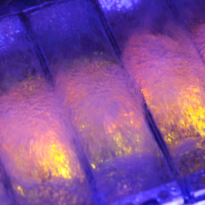
Recently discovered 2D nanomaterials such as graphene, MoS2, WSe2 and other dichalcogenides have shown exceptional properties that will lead to next-gen electronics and photonics devices. Although these materials are in the center of a billion-worth, multidisciplinary research effort, a transfer from the catalytic-growth substrate to an electronic-grade suitable substrate is a necessary step towards industrial applications.
For pushing forward these promising nanomaterials from the lab to the industry, high yield and reproducibility in this crucial step are needed. Our technology can make this happen, providing an automated and scalable method that is compatible with the preexisting industry.
Two areas of major application are nanotechnology (novel materials,conductive coatings,anti-corrosion) and ICT (photonics,spintronics,electronic components and EM shielding).
“2DTransfer enables the industrial applications of two-dimensional nanomaterials, paving the way for disruptive technology”
Market demands
Due to exceptional properties such as high flexibility, unique electronic and optical properties, high transparency or ultrafast charge carriers, two-dimensional nanomaterials are suitable for a wide range of applications. This allows our technology to fulfill different markets.
Some examples for these applications:
Nanotechnology
- Conductive, chemical-resistant coatings
- Heat spreading
- Hydrophobic surface treatments ICT
- Faster consumer electronics
- Internet of things solutions
- Interaction with the environment
- Flexible and transparent devices
Enabling the nanomaterial-solutions journey from the lab to the industry by means of an automated process
Competitive advantages
-
Suitability for brittle, rigid or flexible substrates, not only for flexible substrates as roll-to-roll systems developed by Samsung and Sony.
-
Material quality is not affected by the process.
-
Industrial scalability, both in size and in number of parallel processes.
-
Low implementation cost.
-
Compatible with the current planar technology.
-
Avoid the use of conflict minerals and heavy metals (Sn, In, Pb, Hg, Cd).
-
Enables the implementation of disruptive technology based on nanomaterials.
Development stage
- Concept
- Research
- Lab prototype
- Industrial prototype
- Production
Contact
Contacto 2DTransfer
Alberto Boscá, Fernando Calle
e:
e:
w:http://www.isomgraphene.es/
Contacto UPM
Área de Innovación, Comercialización y Creación de Empresas
Centro de Apoyo a la Innovación Tecnológica – UPM
e: