Molecular Beam Epitaxy (MBE) Team
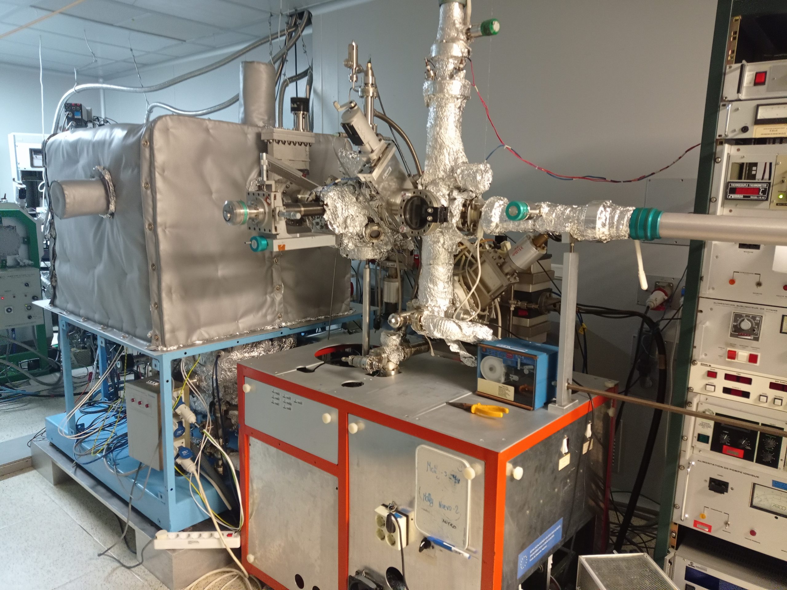
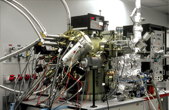
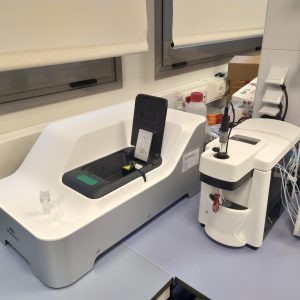
RIBER 32 for As-III-based semiconductors
Using this equipment, layer structures can be made for
semiconductors based on group III arsenides [GaAs(N,Sb),
InGaAs(N,Sb), AlGaAs(N,Sb)], with atomic resolution (individual
atomic layers in various materials) and with highly precise control of
flatness and thickness. This enables quantum
well and quantum dot devices to be made.
Description of the services offered
The equipment enables many different devices to be developed, such as
light emitters (LED, LASER, Single photon emitters), filters,
modulators, diodes, transistors or light detectors. It is the
basic equipment where material is made which is used in the remaining
processes and, therefore, is the beginning of the entire manufacturing chain for
any electro-optical device.
Needs requested and applications
Apart from making light emitters and photodetectors, the equipment is highly suited for use in quantum communications, as it is capable of making light emitting and detecting structures that are essential for this type of communications. Depending on the type of materials used, its wave length in use extends from 620nm up to approximately 20 µm in the IR-visible.
Sector or area of application
Electronics, Optics, Optoelectronics, Quantum communications.
Differential skills
The differential advantage of growth with MBE is that its resolution is +/- 1 atomic layer (approximately +/- 5 nm) It has several systems for monitoring material quality in-situ. Amongst them, one of the highlights is RHEED (Reflection High Energy Electron Diffraction) which enables analysis of the crystal¿s growth facet while progressing and assessing its quality, growth speed and thickness, as well as detecting the appearance of quantum dots on the surface.
Previous references for provision of services
Where it is
ISOM. HTSE for Telecommunications


