


Scientific and technology services
Thickness measurement and optical profiling of thin films
Description of the services offered
Micro and nanometric thickness measurement using thin film reflectance spectra. At the same time, profiling the refractive index of the material forming the film.
Needs requested and applications
Many applications using thin films require specific thicknesses, which is why it is essential to profile them. At the same time, calculating an unknown material’s refractive index can give information about it, and also serve for profiling and optical simulations that need to be carried out on the material.
Sector or area of application
Micro and nano production. Optical profiling.
Differential skills
The equipment used for this service give highly competitive precision measurement, when compared to that available on the market. Furthermore, due to the use of microscope objective lenses, if is possible to measure micrometric areas.
Equipment description
The facilities have different equipment for thin film optical profiling. From the simplest to the most sophisticated. One or the other is offered, depending on the applicant.
Dispersive spectrometer: F20-UV, made by Filmetrics, which is capable of measuring semi-transparent film thicknesses of up to 20 ¿m in reflection. In this case, the spectral window covered is 200 to 1,100 nm, as Filmetrics uses two lamps at the same time ¿one is deuterium and the other is halogen. The equipment’s resolution is 1 nm and the diameter of the beam in the measurement can be 200 ¿m or 2 mm. The measurements are processed using the FilMeasure proprietary system, using measuring formulae depending on the type of measurement to be carried out.
- Optical objective lenses: 4x
- Beam size: large beam (1 mm), reduced beam (200 mm)
- Light source: white light lamp for measurements in VIS-NIR; Possibility of using a UV lamp.
- Power source: Electrical connection.
- Signal acquisition: Spectrometer.
- Extras: Calibration wafer of silicon oxide on silicon. Reference silicon wafer.
- General use of the equipment using the FilMeasure proprietary software.

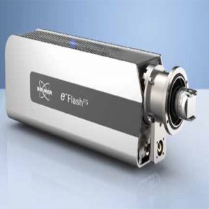
Fourier Transform Infrared and Visible Spectrometer FTIR-VIS: The system has a Michelson interferometer: The measurement obtained is from an interferogram (X, or abscissa, axis contains the various longitudes of the mirror and the ordinates contain the intensity collected by a detector) converted, using Fourier Transform, into a simple reflective or transmission spectrum in the near visible-infrared and medium infrared range. Having previously carried out a simple spectrum of a substrate, when the sample¿s simple spectrum is divided by the reference spectrum, the material’s spectrum is obtained. The equipment is made by Bruker, and uses a tungsten filament that emits near-infrared light and a halogen lamp for the visible. It has a very wide spectral range (from 28000 cm-1 up to 15 cm-1) and a minimum resolution of 0.5 cm-1. The apparatus is connected to a Hyperion 1000 microscope made by the same company, with various objective lenses and magnifications, and a micro-positioning system.
- Optical objective lenses: 4x/15x/36x/40x
- Light source: white light lamp for measurements in VIS-NIR; medium-infrared lamp.
- Power source: Electrical connection.
- Signal acquisition: Various photodetectors (Si, GaP). Obtains the spectroscopic signal with Fourier transform.
- Extras: photomultiplier for the macro function, possibility of external source.
- General use of the equipment using the OPUS proprietary software.


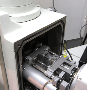
Ellipsometry (N-GAUGE): The ngauge equipment enables reflectometry measurements to be taken depending on the angle of incidence and polarisation on wafers or chips, in sub-micrometric areas, due to the incorporation of a high numerical aperture microscope objective lens (Objective 150, NA 0.95). The measurements can be used to measure the thicknesses and optical properties of materials in thin layers, using the equipment¿s software controller. It can also be used as a conventional optical microscope, via the software controlling one of the cameras (visible light camera).
- Optical objective lenses: 5x, 20x, 50x, 150x.
- Light source: 637 nm laser, white light lamp for the microscope function.
- Power source: Electrical connection.
- Signal acquisition: high resolution monochrome camera, visible spectrum camera for the microscope function.

Request for service
Contact by e-mail, putting ¿PROVISION OF SERVICE¿ in the subject, and the service in question with an approximate description of what is required and the time line in the body of the e-mail.