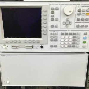

Growth service by Molecular Beam Epitaxy (MBE)
Automated Semiconductor wafers growth with equipment Veeco-GEN10.
Descripción de los servicios que se ofrecen
Growth of semiconductor structures by nanotechnology up to 3 inches.
Needs and applications covered
Semiconductor material wafers with high reproducibility and material quality.
Sector
Semiconductor materials in the photovoltaic, micro and nanoelectronics, optoelectronics industries. Energy, space and electronic sectors.
Cutting-edge characteristics
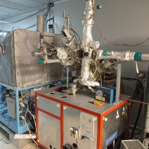
Our MBE is a GEN10 System made by Veeco. Wafers are uploaded automatically in the growth chamber from a cluster chamber than can store wafers ready for their use. If required, the system could run growth recipes to grow 12 wafers without interruption before the system would need to be reloaded with wafers. At present it has the potential to grow III/V compounds based on Al, Ga, As and In using Be an Si as dopants. The system could be upgraded with a second and third growth chambers if the project would demand it. The system counts with a RHEED system to monitor crystal growth and with a Bandit for temperature control during growth. A digital camera is attached to the RHEED and the software made by our engineers is capable of processing the signal of the camera in real time to monitor, for example, RHEED oscillations in order to determine semiconductor growth rates.
The Veeco GEN10 Molecular Epitaxy (MBE) equipment belongs to one of the most advanced generations of MBEs worldwide, and is the first of these characteristics to be installed in a European research center. It has a high degree of automation that facilitates obtaining high reproducibility and repeatability when exploring the behavior of materials based on quantum dots in terms of composition, size, number of layers, etc.
The reactor can be preloaded with 8 wafers and can have three growth chambers simultaneously.
Where we are
Instituto de Energía Solar. Sede: Moncloa.
Avenida Complutense 40. 28040 Madrid. España.
Service Request
Due to the nature of the service, the equipment and the rooms of chemical chambers and clean rooms that are used, it is necessary to carry out in-depth training and have extensive experience in this field. Therefore, although the service may be required by any interested person, it may only be performed by our own personnel. Please contact the person in charge of the service if you are interested in our services.