

Solar Cell Proccesing Service
Solar cell proccesing service and electronic devices manufacturing.
Servicies offered
The manufacturing of electronic devices such as solar cells from semiconductor materials demands the iteration of several technological processes. In the last decade the Instituto de Energia Solar has become a specialist in the manufacturing of devices on different semiconductors (III-Vs, II-VIs) received from several Organizations and Institutions in the framework of national and international research projects.
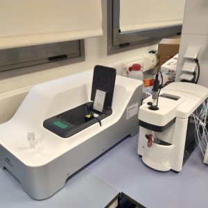
Our manufacturing service has the following capabilities:
- Cleaning and etching: acids, organics, plasma asher, contact layer etching, mesa etching
- Metallization: lift-off, evaporation of n-type and p-type contacts
- Photolitography: Positive and negative resist, photolitography without mask
- Rapid thermal annealing
- Device encapsulation
- Wire bonding
- Dicing
Needs and applications covered
- Processing of semiconductors for companies and other research centers.
- Developing of suitable processing methods for third generation solar cells.
- Consultancy on processing
Sector
Semiconductor materials in the photovoltaic, micro and nanoelectronics, optoelectronics industries. Energy, space and electronic sectors.
Cutting-edge characteristics
Our experience of more than 25 years in manufacturing solar cells, together with an intense activity in the field of innovation creating third-generation solar cells, have made us reliable experts in these processes. We also have the latest technology in our facilities that ensure high quality and reproducibility of the results.
Where we are
Instituto de Energía Solar. Sede: Moncloa.
Avenida Complutense 40. 28040 Madrid. España.
Service Request
Due to the nature of the service, the equipment and the rooms of chemical chambers and clean rooms that are used, it is necessary to carry out in-depth training and have extensive experience in this field. Therefore, although the service may be required by any interested person, it may only be performed by our own personnel. Please contact the person in charge of the service if you are interested in our services.