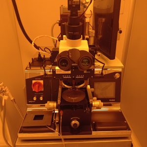

High resolution electron beam lithography
Electron beam lithography equipment enabling designs of less than 50 nm to be carried out. The beam has a minimum diameter of 2 nm. The system has also been recently updated with a high precision interferometric stage.
Description of the services offered
– Production of all kinds of nanometric devices using electron beams.
– Training in the use of electron beam lithography
Needs requested and applications
It is increasingly necessary to produce devices with nanometric sizes. Devices of these sizes have different properties from micro-millimetric devices. Their high aspect ratio means that they are more sensitive devices that consume less energy.
Sector or area of application
Nanotechnology, electronics, optoelectronics, photonics, energy, spintronics.
Differential skills
It is the equipment with the highest resolution for producing nanometric devices in the country. It is up-to-date with the very best features and is the testing and demonstrating bench for the Japanese company in Europe.
Previous references for provision of services
National projects, European projects, international projects.
Where it is
ISOM. HTSE for Telecommunications