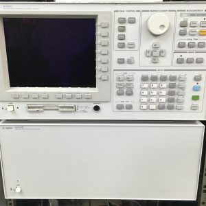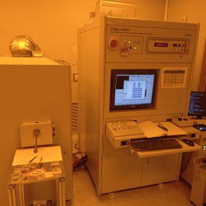
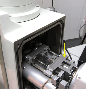
High resolution lithography
The equipment lithographs all kinds of designs on positive and negative resins, on up to 4 inch wafers. The designs carried out can be up to 500 nm due to the 240 nm ultraviolet lamp.
Description of the services offered
– Developing lithographs with conventional masks on flat wafers or substrates. Designing a specific mask for an application. Positive and negative lithography. Device contact using lithography
– Training in the use of lithographic techniques
Needs requested and applications
This kind of service is used to make devices from 0.5 micron to a few millimetres. The applications are highly varied depending on the device to be made
Sector or area of application
Electronics, optics, optoelectronics, magnetic devices
Differential skills
The lithographic equipment is in a White Room which is certified as ICTS – Singular science and technology infrastructure. This means that it has extremely high air quality with hardly any contaminant particles, due to the HEPA filters. The White Room technicians have extensive experience in mask design and lithography on various materials, as well as device interconnection.
Previous references for provision of services
Where it is
ISOM. HTSE for Telecommunications